Home»Blog»Design for Manufacturing (DFM) for PCBs: Electronic Boards That Are Easier to Build
·by Giorgio Minguzzi·7 min read
Design for Manufacturing (DFM) for PCBs: Electronic Boards That Are Easier to Build
A smaller component is not always the better choice. DFM connects PCB layout, SMT assembly, component availability and series production.
Choosing a component for an electronic board does not only affect circuit performance. It can change the assembly process, the inspections required and the stability of series production.
A well-designed board has to meet its functional requirements and keep the process stable as it moves from CAD to the SMT line. Compact layouts and miniaturised components may be necessary, but every choice affects placement, solder paste printing, inspection, testing and the future availability of the component itself.
Design for Manufacturing for PCBs, or PCB DFM, assesses manufacturability during development, while changing a decision is still relatively easy. For engineering and purchasing teams, PCB DFM links performance, component availability, process repeatability, industrialisation lead times and the total cost of the board.
In short, DFM helps you choose the complexity you actually need: if a 0201 is required, the process adapts to it; if a 0402 or 0603 will do the job, the larger package gives you more production margin.
What Design for Manufacturing means for PCBs
Design for Manufacturing (DFM) covers the design choices that make a product compatible with reliable, repeatable production processes over time. For electronic boards it applies both to bare PCB fabrication and to the subsequent assembly of components, which is why the term DFMA (Design for Manufacturing and Assembly) is also used.
Designing a PCB for production means checking the layout against the real capabilities of the line. It looks at footprints, clearances, component orientation and density, solder paste volumes, test access and compatibility with inspection processes. The analysis helps decide which complexity to keep because the product needs it, and which to rethink because it brings no measurable benefit.
When the package changes the production process
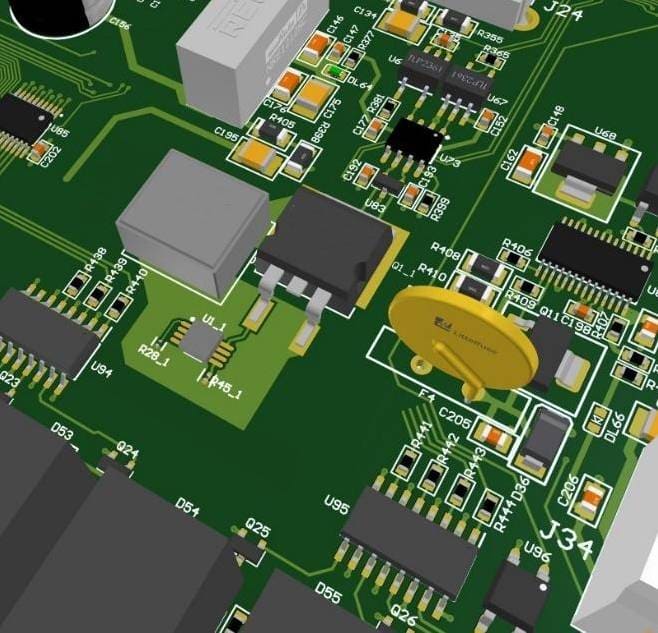
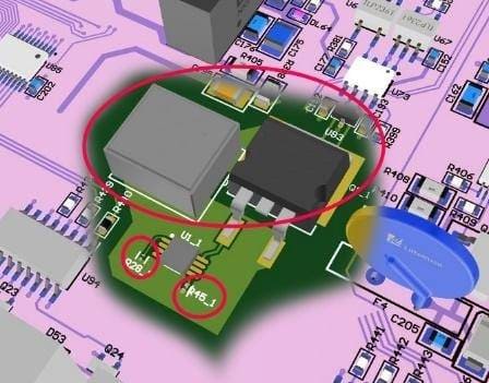
The board shown in these images is a practical example. Power components, with significant thermal mass and joints that need adequate solder volumes, sit only a short distance from passive components in 0201 packages. The layout can be assembled, but it places very different process requirements in the same area.
A 0201 package allows a high degree of miniaturisation and can be the right choice when board space or electrical performance demands it. Its small size, however, calls for close attention to stencil aperture design, solder paste deposition, placement and thermal profile stability. In the same area, a larger component may need a different paste volume and absorb heat differently during reflow.
Why the smallest component is not always the best
A modern SMT line can handle 0201 components, stencils of different thicknesses, optimised thermal profiles and advanced inspection.
Production capability does not make design discipline unnecessary, though: was that package really needed? If a 0402 or 0603 meets the same requirements without changing footprint, performance or mechanical constraints, the larger package can offer a more favourable process window.
The rule of thumb at Electra is to choose the largest component that is compatible with the real requirements of the design.
Miniaturisation remains the right choice when it answers a space constraint, an electrical performance target or a mechanical requirement.
In other cases, a less aggressive package can reduce sensitivity to variations in printing, placement and reflow.
The effects on SMT assembly and inspection
Having very small components alongside components with high thermal mass may require specific work on the PCB assembly process.
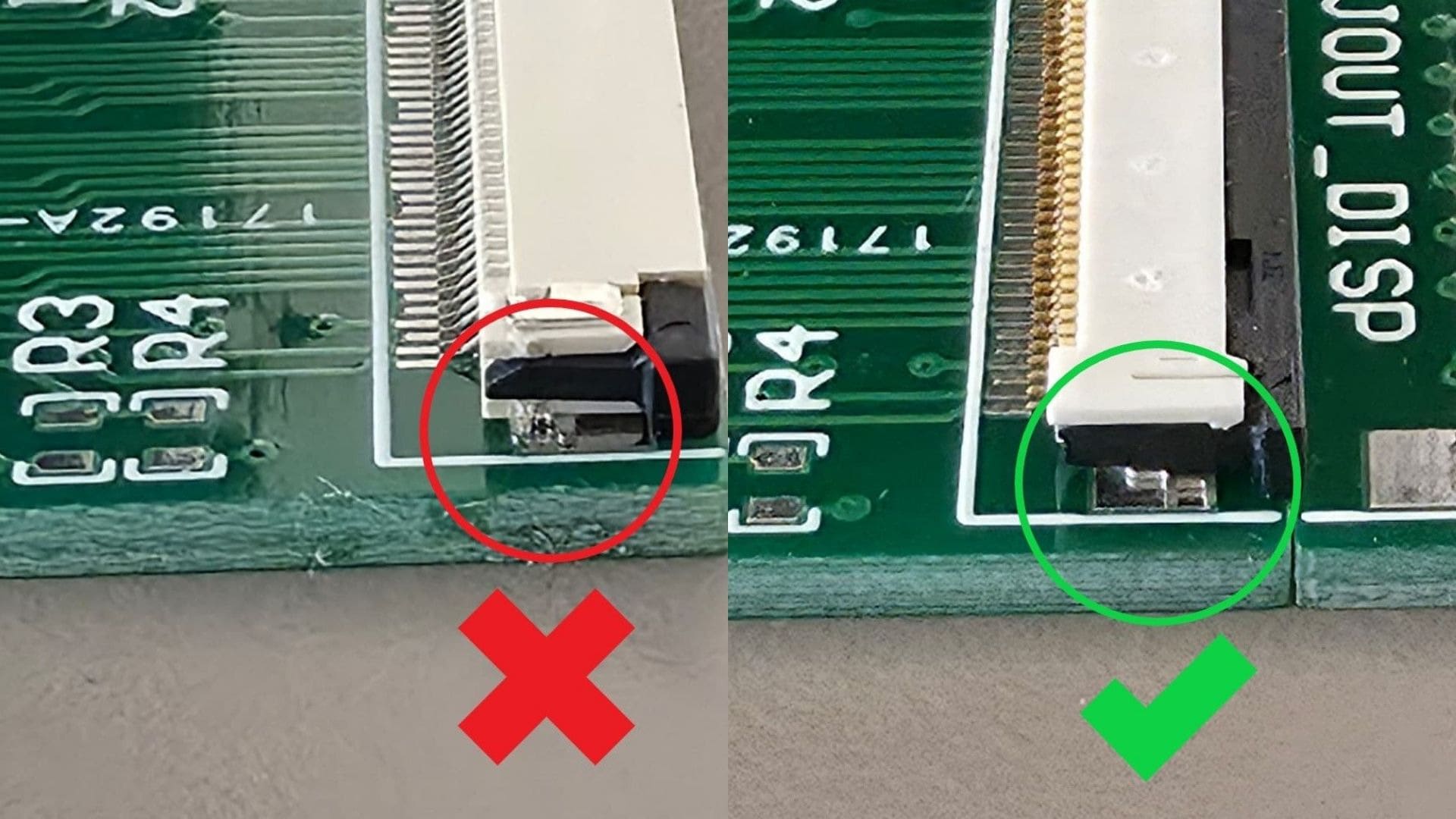
Stencil apertures must deposit paste volumes consistent with the pads and terminations. The reflow profile has to bring the whole board within the correct process windows, taking the different thermal responses into account. Orientation, clearances and mechanical support of the PCB can also affect repeatability.
Inspection methods should be chosen according to the board and the joints that need to be verified.
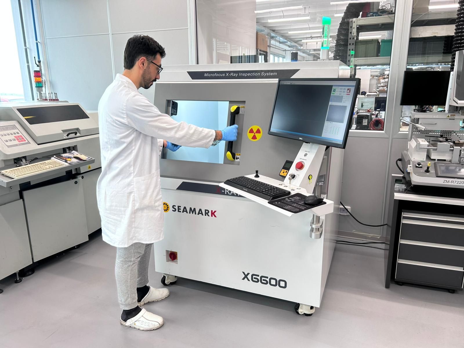
Automated optical inspection (AOI) checks visible features and many assembly defects. X-ray inspection becomes useful when the geometry of the component or the joint does not allow full optical inspection, for example with hidden connections. The inspection plan therefore depends on the design as a whole, not simply on the presence of a 0201 package.
Why DFM matters to engineering and purchasing
For engineering teams, designing to DFM criteria means fewer late corrections and layout choices that are checked against the process that will build them. For purchasing teams, it means assessing the bill of materials in terms of availability, compatible alternatives, life cycle and production impact. Unit price and footprint alone do not describe the real cost of a choice.
A component can look attractive in the catalogue and still require a more demanding process, additional inspection or less flexibility when qualifying alternatives.
Bringing design, purchasing and production together makes it possible to consider these factors before the production files are released. The result is a more robust BOM and a smoother transition from prototype to medium or high volumes.
From CAD to the SMT line in one process
At Electra, electronics and PCB design and production work closely together. The consequences of a choice made in CAD can be seen directly at solder paste printing, pick and place, reflow and inspection. This continuous exchange means manufacturability is addressed during development and industrialisation, rather than being left to the production stage.
Electra’s experience, built on more than 5 million boards produced and 2.5 billion components placed, links design decisions to their industrial implementation. Electra’s PCBA manufacturing covers thermal profiling, solder paste printing, placement, reflow, 3D optical inspection and X-ray inspection. These technologies make it possible to assemble complex PCBs. DFM ensures they are used within a process built around the product’s real needs, rather than turning an unnecessary choice into recurring complexity for every batch.
Involve production before release
The most useful time for a DFM review is before the layout is considered final. Even a short review can highlight issues with packages, clearances, stencil design, thermal management or inspection. Correcting them at the design stage protects the work already done and prepares the board for the repeatability that series production requires.
Electra supports companies in the development, industrialisation and production of PCBs and electronic equipment. To assess the manufacturability of a new design or an existing board, contact the Electra team.
Frequently asked questions about Design for Manufacturing for electronic boards
Here are some of the questions our customers ask most often on this topic.
What is DFM for PCBs?
PCB DFM is the set of criteria used to make a printed circuit board and its assembly compatible with reliable, repeatable production processes. It reviews the design before release, taking into account layout, components, stencil, reflow, inspection and testing.
When should 0201 components be used?
0201 components are appropriate when miniaturisation, density or electrical performance justify them. If larger packages meet the same requirements, comparing alternatives such as 0402 and 0603 with the 0201 helps strike the best balance between footprint and production margin.
Is a smaller PCB always cheaper?
Not necessarily. Reducing the size can cut material usage, but higher density may require smaller components, more demanding processes and additional inspection. Cost should be assessed across the whole industrialisation and production cycle, not just on the area of the circuit board.
When should the electronics manufacturer be involved?
The manufacturer should be involved before the layout and bill of materials are released. At this stage it is still possible to correct packages, clearances, orientations and process choices without causing rework on prototypes or late changes to documentation.
What inspection does a complex SMT board need?
The inspection plan depends on the components, geometries, product requirements and process risks. AOI, X-ray inspection and functional testing do different jobs and should be selected according to what needs to be verified, rather than automatically linking a single package to every available check.
What is the difference between a PCB and a PCBA?
A PCB is the printed circuit board before components are mounted. PCBA refers to the assembled board, complete with soldered components. A DFM review should consider PCB fabrication and, together with DFA criteria, the requirements of the subsequent assembly.
Does DFM also cover the bill of materials?
Yes. Manufacturability also depends on component availability, qualified alternatives, life cycle and sourcing constraints. Reviewing the BOM together with the layout allows engineering, purchasing and production to make consistent decisions before series production.
AOI, X-ray inspection, ICT and functional testing are different but complementary checks. Here is how they improve reliability, traceability and quality in PCBA manufacturing.